Nanolithography by selective chemical vapor deposition with an atomic hydrogen resist
We report the fabrication of Al nanostructures using selective chemical vapor deposition (CVD) growth and an atomic hydrogen resist. A scanning tunneling microscope is used to pattern the hydrogen terminated surface by local removal of hydrogen atoms. The high selectivity of the CVD process limits Al growth to the uncovered regions. We demonstrate the fabrication of Al features as small as 2 nm.
_______________________________________
Lyding et al. demonstrated the atomic scale desorption of hydrogen from a monohydride covered Si(001)-(2×1) surface using an STM (1,2). The difference in reactivity between the hydrogen terminated and bare silicon areas opens possibilities for nanoscale fabrication. Pattern transfer was demonstrated by evaporation (3), by oxidation and by selective chemical-vapor deposition (CVD) (4), on the STM patterned atomic hydrogen resist. In this paper, we show that the selective CVD process can be used to form Al nanostructures on Si surfaces with an atomic H resist. The use of selective CVD provides an improved realization of the atomic resist process, resulting in a useful process for the fabrication of nanoscale structures.
Adams et al demonstrated selective growth using a CVD precursor, Fe(CO)5 successfully on a patterned hydrogen terminated surface (4). We will use an Al precursor, Dimethylaluminum hydride (DMAH, Al(CH3)2H), a promising new chemical precursor because of its stability, low carbon contamination, and ease of introduction. Al CVD using DMAH has been extensively studied over the last few years (5).
We have studied the initial stages of Al CVD growth from DMAH on the bare Si(001) surface (6). At room temperature, DMAH adsorbed intact on the bare Si surface. At temperatures above 120°C, Al deposition began. Clean Al growth was observed for substrate temperatures between 150 and 300°C. By contrast with bare Si, we find that DMAH does not stick on a room temperature monohydride terminated Si surface. Furthermore, no aluminum deposition is observed on monohydride surfaces up to 300 °C. This indicates that DMAH can provide high selectivity between bare and monohydride terminated Si(001) surface at temperatures between 150 and 300°C (7).
In fact, this selectivity can be used in a selective CVD nanolithography process. Figure 1 (a) shows a clean monohydride terminated Si surface before patterning. Figure 1 (b) shows a 50 nm square of bare silicon from which the hydrogen has been removed by scanning at increased current and voltage. In Fig. 1 (c) we show the initial stages of selective Al growth on the clean patterned area. A 0.5 langmuir dose of DMAH produces a uniform distribution of dilute Al dimer rows in the patterned region (8). Further deposition uniformly fills the patterned region with nanometer sized aluminum clusters, as shown in Fig. 1 (d). However, the monohydride terminated region remains clean throughout the pattern transfer.
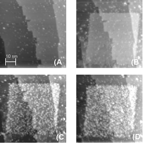
Fig. 1. STM images of aluminum deposition procedure. (A) Initial Si(001) monohydride surface. (B) A 50 nm bare silicon square is patterned by removal of H. (C) Initial Al deposition (0.5 L) shows good selectivity and uniform growth. (D) Continued deposition (4 L) approaches a thin Al film.
It is important to note that there is no aluminum growth enhancement along the border between the silicon and hydrogen terminated regions in Fig. 1. Such an enhancement was observed by Shen et al. for aluminum delivered by MBE (3). It was attributed to free aluminum on the hydrogen terminated surface diffusing to and sticking on the bare region. The DMAH deposits the Al only on the bare silicon regions and the selectivity is better than 250 to 1 for the fabrication process.
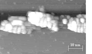
Fig. 2. STM image of a thick aluminum wire. The wire results from a 1000 L dose of DMAH. It measures 10 to 15 nm wide and 1 to 4 nm thick.
This complete selectivity allows fabrication of thick, continuous Al wires such as that shown in fig. 2. This wire is 1 to 4 nm thick and results from a 1000 L dose of DMAH. Runaway growth of the larger Al clusters is evident.
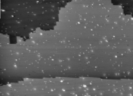
Fig. 3. STM image of an Al nanostructure fabricated using chemical vapor deposition with an atomic hydrogen resist. The line width is less than 4 nm and the height is 0.3 - 0.5 nm. This animation shows the surface after each of the steps in the process. First the bare Si surface is mono-hydride terminated, next the hydrogen is removed with the STM tip to spell "Al CVD", and finally the surface is dosed with DMAH which fills in the lettering with aluminum.
Our lithography method combines the high selectivity of the CVD precursor DMAH with the precision of an STM patterned hydrogen resist. Sizes as small as 2 nm can be achieved. In Fig. 3, an Al wire thickness of 0.3 to 0.5 nm is produced by a 20 L dose of DMAH. The wires are clearly granular at the early stages of growth. However, we expect that for thicker films, the wires should approach the high quality of CVD grown thin metal films (7). Therefore, we are optimistic that these films can be used for fundamental studies of metallic wires and fabrication of useful nanostructures.
We will now consider the origin of this strong selectivity. The Si(001) – (2 × 1) reconstructed surface is composed of pairs of silicon atoms, each of which are joined by a strong s-bond and a weak p-bond. The presence of the p-bond, only 0.9 eV below the Fermi level, makes this a highly reactive surface (9), on which the DMAH molecules are able to dissociate and deposit Al. In the case of the hydrogen terminated surface, the p-bond is replaced by two strong Si - H s-bonds and the surface is passivated (10). Thus, the DMAH is unable to chemically bond or dissociate on this surface.
We have demonstrated the selective growth of Al using a nanolithographic technique that is capable of fabricating structures with dimensions on the order of a few nanometers. As selective deposition of Fe has already been demonstrated, we expect that selective deposition of gold, nickel and other metals will be possible (11). This will permit applications in fundamental studies of the conductivity of nanoscale wires, superconductivity and magnetism, as well as the fabrication of individual nanoscale devices.
References and Notes
(1). T-C. Shen,
C. Wang, G. C. Abeln, J. R. Tucker, J. W. Lyding, Ph. Avouris,
and R. E. Walkup., Science 268, 1590
(1995).
(2). J. W. Lyding, T. -C. Shen,
J. S. Hubacek, J. R. Tucker, and G. C. Abeln, Appl. Phys.
Lett. 64, 2010 (1994).
(3). T.-C. Shen, C. Wang, and
J. R. Tucker, Phys. Rev. Lett. 78, 1271 (1997).
(4). D.P. Adams, T. M. Mayer,
and B. S. Swartzentruber, Appl. Phys. Lett. 68
2210 (1996); J. Vac. Sci. Technol. B 14, 1642 (1996).
(5). K. A. Littau, R. Mosely,
S. Zhou, H. Zhang, and T. Guo, Microelectronic Engineering
33, 101 (1997).
(6). Fundamental
studies of Chemical Vapor Deposition Growth on Si(001)
(7). The diffusion of the
adsorbed hydrogen limits the process to temperatures below 250
°C to avoid degradation of the patterning. See J. H. G. Owen, D.
R. Bowler, C. M. Goringe, K. Miki, and G. A. D. Briggs, Phys.
Rev. B. 54, 14153 (1996).
(8). G. Brocks, P. J. Kelly,
and R. Car, Phys. Rev. Lett. 70, 2786 (1993); J. Vac. Sci.
Technol. B 12, 2705 (1994); J. Nogami, A. A. Baski, and C.
F. Quate, Phys. Rev. B 44,1415 (1991).
(9). J. A. Appelbaum, G. A.
Baraff, and D. R. Harmann, Phys. Rev. B. 14, 588 (1976);
R. J. Hamers, Ph Avouris, and F. Bozso, Phys. Rev. Lett.
59, 2071 (1987).
(10). Y. W. Michael, J.
Bronikowski, and R. J. Hamers, Surf. Sci. 311, 64
(1994).
(11). The Chemistry of Metal
CVD, T. Kodas, and M. Hampden-Smith, Ed.(VCH, Weinheim, 1994).
We would like to thank Craig Moody and Dan Columbo for their assistance and Wayne Gladfelter for valuable discussions. The Schumacher Co. kindly supplied us with the DMAH. We would also like to thank the NSF for supporting this research through grant DMR-9508937.
Jump to
Hot STM
Labs
Fundamental
studies of Chemical Vapor Deposition Growth on Si(001)
Copyright 1998 by the Regents of the University of Minnesota, Dept. of Physics & Astronomy. All rights reserved.