![]()
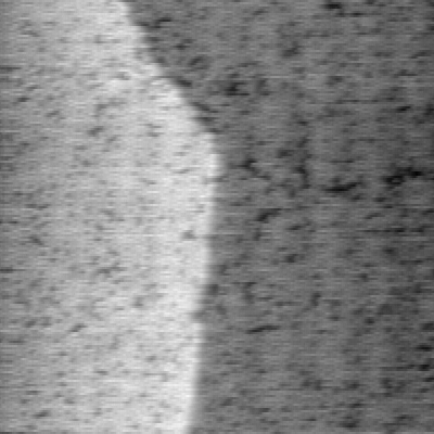 |
Fig. 1 An early image of the Si(111)-7 X 7 reconstructed surface taken in vacuum by the Fast STM. Size= 600 × 600 Å ; Scan Rate= 81,840 Å/s..
Motivation
to Build a High Speed STM
For almost any application of an STM, increased
speed is a definite advantage. In the case of data
storage/recall, increasing the speed brings the processes one
step closer to being commercially applicable; the same holds for
nanolithography. In our realm of interest, here at the Hot STM
Labs, increased speed means we can study surface dynamics at
elevated temperatures with better time resolution. As the
scanning rate approaches the rates of fundamental processes
(particle diffusion, nucleation, etc.) we become capable of
actually capturing these processes in real time movies. In
particular, we have developed this tool for studying the
complexities of Chemical Vapor Deposition (CVD) growth.
Mechanical
Design of High Speed STM
In developing a high speed STM two tricky issues had to be
addressed: how to make the tip’s elevation above the sample
(it’s Z position) responsive to the rapidly changing
topology over which it scans, and how to avoid operating in
resonance with the apparatus. Addressing the latter issue, we
chose the materials (high stiffness & low mass) and
dimensions (small) of our mechanics so as to push the resonance
frequency above our scan frequency. As for the first issue, we
have followed the prescription of H. J. Mamin et al, J. Appl.
Phys. 75, 161 1994, and split the Z-scanning task in half.
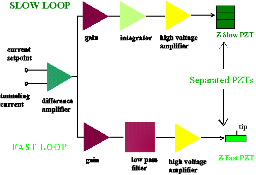 |
Fig. 2 Schematic of the separate circuitry for controlling the fast and slow Z-motion of the tip. Note that the Fast branch of the loop has does not have an integrator slowing down its operation, instead it simply has a low pass filter to keep the signal clean. Not having an integrator means that, without receiving feedback from the Slow branch (a conventional STM's circuitry), the Fast branch could only respond to instantaneous changes in surface topography.
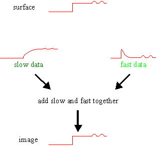 |
Fig. 3 Illustration of how the Slow and Fast branches of the Z control loop work in concert to reconstruct a complete image of the scanned surface. The Fast branch has been optimized to provide a quick response to the rapidly varying topography over which the tip scans. Meanwhile the Slow branch, with its sluggish (conventional) response, follows to handle the large scale elevation changes. Together they give an accurate picture of both large and small scale features on the scanned surface.
In the Dual scan unit scheme, we have a slow branch which is optimized for slow, low noise response with high gain. This is the piezo and circuitry that respond to our scanning on one plane or the terrace above. This leaves it to the fast branch to provide the high frequency response as the tip scans across, say, a single atom feature. By so splitting the task, we can optimize the design of both loops for their respective tasks.
Prototype High Speed STM in Air
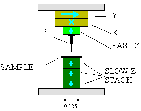 |
Fig. 4 Prototype tip and piazo arrangement. In this version of the High Speed STM the Slow and Fast Z piazos are on opposite sides of the sample and tip. Fig. 5 shows the arrangement for the UHV Hot version.
The first step in developing our high speed UHV
STM was putting together a prototype system for operation in air.
With this we were able to test the dual scan scheme’s gains
in speed and the mechanical design’s control of undesirable
resonant behavior. Here we also tested a high speed amplifier
design that was developed by B. Michel et al, Ultramicroscopy
42-44 (1992).
The system tested well. We were able to take
atomic resolution images with tip speeds up to 1,000,000 Å/s and
a frame rate of 15Hz; though, at these extreme speeds, some image
resolution was sacrificed. Featured in
these movies is a (111) plane on a ball of Au. Gold made a
particularly good subject for study in air because it is
relatively non-reactive, and single-atomic height terraces are
formed when a tip of gold wire is melted and allowed to cool
naturally into a single crystal ball.
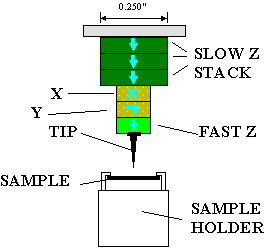 |
Fig. 5 UHV Hot tip and piazo arrangement. In this version of the High Speed STM the Slow and Fast Z piazos are on the same side of the sample and tip. This allows for sample heating without inducing a state transition in the Slow Z Stack piazos. Fig. 4 shows the arrangement for the Prototype version.
Though the prototype system performed
exceptionally well in air and proved that the high speeds are
achievable, a few modifications had to be made to allow for UHV
and hot sample operation. The high speed amplifier has to be made
vacuum worthy or replaced, since the closer the amplifier is to
the tip the better, and that means the amplifier should be in the
vacuum chamber. Also the piezo stack beneath the sample (that
which is responsible for slow Z response) has to be moved to join
the other piezos behind the tip. This is because the sample will
often be at temperatures above the curie point of the piezo, and
so a piezo in thermal contact with the sample is unacceptable.
With these design modifications, some speed has been sacrificed
in order to maintain the atomic resolution as is present in Fig. 1.
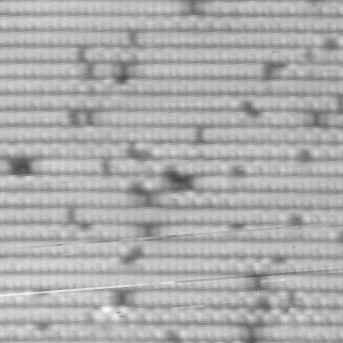 |
Fig. 5 Taken from a 200 Å × 200 Å image of a defect ridden Si(001) - 2×1 reconstructed surface Acquired at 20,000 Å/sec.
With more moderate tip velocities of around 20,000 Å/sec., the Fast STM is displays resolution that rivals that of a conventional machine running at about 1/10th the speed.
The dual Z-scan unit has proven itself with the exceptional performance of our Prototype STM operated in Air.
The modified system for UHV Hot operation still shows high performance with atomic resolution
The UHV STM has been used to study atomic diffusion, molecular adsorption, CVD, and nanofabrication.
This work has been supported by NSF grants DMR 950637 and DMR 9300729
![]()
Jump to
Copyright 1996 by the Regents of the University of Minnesota, Dept. of Physics & Astronomy. All rights reserved.