
 |
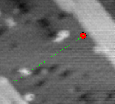
Fig. 1. Tracking a Si dimer along a row on the Si(001) surface at 423K. The dimer's location is sampled at a rate over 1kHz. In this figure, every 500th location is marked by a green dot and the dimer's current location is shown as a red ball. In an animation of this image, the dimer can be seen to jump from site to site, leaving concentrations of green dots spaced evenly by one lattice constant.
A new tunneling microscopy technique has recently been applied to the studies of surface processes on the Si(001) surface. Rather than rastering the tip over an area on the order of 400 × 400 Å in order to construct an image of that area, the tip is dithered in a small (~5 Å diameter) circle. Through the use of a feedback loop, this scan-circle can be locked onto a surface feature. Sampling the feature's location over 1000 times per second, the tip tracks the feature's motion. By not devoting scan time to imaging a large surface area, tracking gains over 1000 fold in time resolution of a single feature's dynamics, but sacrifices information about the dynamics of the surrounding surface. In applications such as the study of a diffusion across a relatively stable surface, this tradeoff is more than acceptable: Around 480K, we are able to observe a silicon dimer's every hop from site to site. By studying hop rates we can now better measure barriers to different paths. Similarly, we can learn much about other dynamic processes such as defect diffusion and step-edge fluctuations.
Applying the tracking technique to studies of Si dimer diffusion on the Si(001)-2 × 1 surface has enabled us to resolve individual diffusive events. Studying these events has allowed us to set the activation energy for diffusion of a dimer along a substrate dimer row at 1.09± 0.05 eV and along the trough at 1.27 ± 0.08 eV, and to place a lower bound of 1.40 eV on the activation energy for dimer dissociation. We have also observed the free energy of a dimer to decrease by 32 ± 2 meV at a site adjacent to a type-A edge.
Fig. 2. One Dimensional illustration of Tunneling Current vs. Slope. With the tip executing small circular orbits in the plane above the sample, the local slope of the sample surface can be detected. This information can then be used in a feedback loop to drive the tip "uphill".
Fig. 3 An illustration of the tip moving "uphill" to a prominence on the sample surface.
The tracking technique was introduced by Pohl & Möller in 1988 and was first applied to the study of Si dimers on Si(001) by Swartzentruber in 1995. It makes use of a feedback loop which causes the scanner's tip to always move "uphill." The tip is set to scan in a tight (~5 Å diameter) circular orbit at a constant elevation. As is illustrated in figure 2, the slope of the surface within that orbit determines the phase relationship between the scan cycle and the tunneling current. By comparing these phases, "uphill" and "downhill" can be discerned, and the tip can be moved accordingly. This means that if a tip's scan-orbit passes over a prominence, such as a dimer, the tip will move "uphill" to it as is shown in Fig.3. As long as its motions are slower than the tip's orbit, the tip can track its diffusion across the silicon surface.
Jump to
Hot STM Labs
Piecewise Diffusion
of the Silicon Dimer
Dimer Dissociation and Step-Edge
Interactions
Hydrogen
Diffusion