
 |
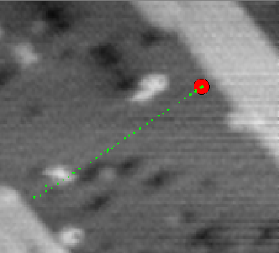
Fig. 1. Tracking a Si dimer along a row on the Si(001) surface at 423K. The dimer's location is sampled at a rate over 1kHz. In this figure, every 500th location is marked by a green dot and the dimer's current location is shown as a red ball. In an animation of this image, the dimer can be seen to jump from site to site, leaving concentrations of green dots spaced evenly by one lattice constant.
![]()
![]()
A new tunneling microscopy technique has recently been applied to the studies of surface processes on the Si(001) surface. Rather than rastering the tip over an area on the order of 400 × 400 Å in order to construct an image of that area, the tip is dithered in a small (~5 Å diameter) circle. Through the use of a feedback loop, this scan-circle can be locked onto a surface feature. Sampling the feature's location over 1000 times per second, the tip tracks the feature's motion. By not devoting scan time to imaging a large surface area, tracking gains over 1000 fold in time resolution of a single feature's dynamics, but sacrifices information about the dynamics of the surrounding surface. In applications such as the study of a diffusion across a relatively stable surface, this tradeoff is more than acceptable: Around 480K, we are able to observe a silicon dimer's every hop from site to site. By studying hop rates we can now better measure barriers to different paths. Similarly, we can learn much about other dynamic processes such as defect diffusion and step-edge fluctuations.
Applying the tracking technique to studies of Si dimer diffusion on the Si(001)-2 × 1 surface has enabled us to resolve individual diffusive events. Studying these events has allowed us to set the activation energy for diffusion of a dimer along a substrate dimer row at 1.09± 0.05 eV, and place a lower bound of 1.40 eV on the activation energy for dimer dissociation. We have also observed the free energy of a dimer to decrease by 32 ± 2 meV at a site adjacent to a type-A edge.
![]()
Fig. 2. One Dimensional illustration of Tunneling Current vs. Slope. With the tip executing small circular orbits in the plane above the sample, the local slope of the sample surface can be detected. This information can then be used in a feedback loop to drive the tip "uphill".
Fig. 3 An illustration of the tip moving "uphill" to a prominence on the sample surface.
The tracking technique was introduced by Pohl & Möller in 1988 and was first applied to the study of Si dimers on Si(001) by Swartzentruber in 1995. It makes use of a feedback loop which causes the scanner's tip to always move "uphill." The tip is set to scan in a tight (~5 Å diameter) circular orbit at a constant elevation. As is illustrated in figure 2, the slope of the surface within that orbit determines the phase relationship between the scan cycle and the tunneling current. By comparing these phases, "uphill" and "downhill" can be discerned, and the tip can be moved accordingly. This means that if a tip's scan-orbit passes over a prominence, such as a dimer, the tip will move "uphill" to it as is shown in Fig.3. As long as its motions are slower than the tip's orbit, the tip can track its diffusion across the silicon surface.
![]()
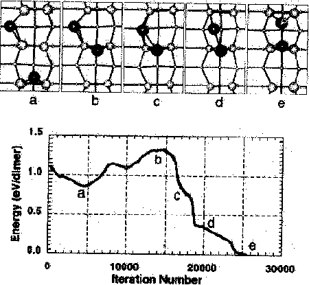
Fig. 4. The dissociation pathway considered by Yamasaki et al.While this depicts dimer formation, the same pathway could be followed in reverse for dimer dissociation. (Reproduced from Yamasaki et al.)
The population of dimers on the silicon surface depends on the activation energy for dimer dissociation. It is therefore important to determine the dissociation energy in order to evaluate dimers' importance in processes under different surface conditions. The theoretical calculations of Yamasaki et al. and Brocks et al. have addressed dissociation. Considering the pathway shown in Fig. 4, Yamasaki et al. have applied Car-Parinello modeling to estimate an activation energy of 1.33 eV.
Experimentally, we can set a lower bound on the dimer dissociation energy by observing a dimer which does not dissociate in time t. The observation time can be related to an energy bound by applying the Arrhenius relation,
Here R is the rate of dissociation, E is the associated activation energy, and v=1013Hz is the assumed attempt frequency. Not seeing a dissociation for time t implies that R<1/t, or
From conventional STM movies at 500 K for 4860 s we found a relatively height bound for E. However, conventional scanning requires that the tip spend only a small fraction of its scan-time over the dimer, so there is the possibility of a dimer's dissociation and reformation going undetected. Nearly continuous observation of a dimer is necessary to minimize this possibility. This is a good application for the tracking technique. By tracking a dimer at 423 K for 8640 s, we find E>1.40eV with a 95% confidence.
![]()
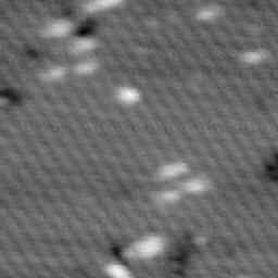 |
Fig. 5. Silicon (001) 2 X 1 Reconstruction with a Diffusing Dimer. As can be seen in this image (and is discussed in greater detail elsewhere) the cleaved surface reconstructs to form parallel rows. Dimer diffusion is predominately along the rows, making the system nearly one-dimensional. The movie from which this image is taken may be viewed as an animated GIF. Unlike many of our other images, this is an empty state image, so the surface rows appear dark and the troughs appear bright.
Fig. 6. One Dimensional Schematic of Barrier to Diffusion. Because of the strong anisotropy of the Si(001) reconstructed surface, diffusion is strongly one dimensional.
The animation of Fig. 5 shows the diffusion of a dimer (the white spot near the center of the image.) As can be seen in the animation, the dimer's motion is restricted to one dimension, along the substrate dimer rows. Fig. 6 is a schematic of the energy contour along a row. A thermal activation of ED is necessary for the dimer to hop from one well to the next. Tracking a dimer as it diffuses across a silicon surface allows the determination of dimer diffusion activation energy by again applying the Arrhenius relation.
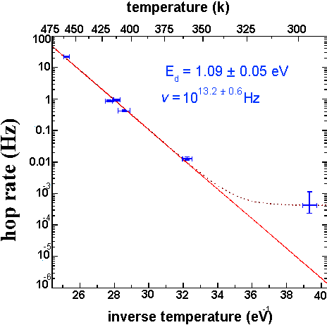
Fig. 7 Arrhenius plot for determining diffusion activation energy. According to the Arrhenius relation R=ve-ED/KT for any simple thermally activated process. By observing hop rates at several temperatures we are able to determine values for both the activation energy, ED, and the attempt frequency , v. Note: at low temperatures the tip induced diffusion rate becomes significant; this is responsible for the large diffusion rate observed at room temperature.
By taking transition rate measurements at different sample temperatures, the plot in Fig. 6 has been constructed. From the slope of this plot, an activation energy for dimer diffusion is found to be 1.09 ± 0.05 eV.
It is worth noting that while the hop rate is plotted logarithmically, the temperature is not, so the plot is relatively unforgiving of errors in temperature measurements. For this reason we performed a temperature calibration using the known melting point of indium and we employed an iterative temperature equilibration method for measuring sample temperature.
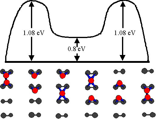
Fig. 8. The diffusion pathway considered by Yamasaki et al. They found the corresponding activation energy to be in excellent agreement with the value we have measured experimentally.
Swartzentruber has used the tracking technique to obtain a value of 0.94 ± 0.09 eV; the discrepancy between our two values is probably due to a temperature measurement error. In excellent agreement with our findings, Yamasaki et al. recently found 1.08 eV by ab initio calculations for the diffusion pathway shown in Fig. 8.*
![]()
Central to any epitaxial growth model is an understanding of how the adsorbate in question interacts with islands, steps, and other surface features. As can be observed in conventional STM movies, it is not sufficient to assume that an adsorbate sticks with unit probability when it meets an atomic-height step; one must consider these interactions in more detail.
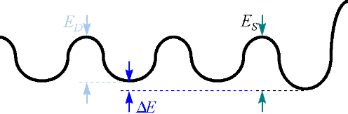 |
Fig. 9. Schematic of the 1D potential for dimer motion along a substrate dimer row that terminates on the right at a type-A step.
We have observed dimers trapped between and on
top of surface islands (of single atomic height). We have also
observed that dimers spend a longer period of time in sites at
the bottom of step edges. These observations indicate the
existence of edge-site barriers and wells, as are depicted in
Fig. 8. The hop rates across the potential barriers in Fig. 9 are
related to those barriers by the Arrhenius relation: ED=KTln[vD/RD]
and ES=KT ln[vS/(2 RS)],
or ES - ED
= kT ln [RDvs/(2RSv
![]()
There can be a great disparity between a conventional STM's imaging rate and specific surface process rates. This limits the applicability of conventional STM techniques to surface dynamics studies. The tracking technique narrows the observation and process rate disparity by sampling only the immediate vicinity of a feature. By applying this technique to studies of Si dimer diffusion on the Si(001)-2 × 1 surface, we have resolved individual diffusive events. Studying these events has allowed us to set the activation energy for diffusion of a dimer along a substrate dimer row at 1.09 ± 0.05 eV, and place a lower bound of 1.40 eV on the activation energy for dimer dissociation. We have also observed the free energy of a dimer to decrease by 32 ± 2 meV at a site adjacent to a type-A edge. This tracking technique may be applied to the study of number of surface features and adsorbates on a variety of surfaces. As with our application to Si dimers a Si surface, the tracking technique promises to provide time resolutions of single feature processes that are unattainable by current conventional STM techniques.
![]()
G. Brocks, P. J. Kelly, and R. Car. Phys. Rev. Lett. 66, 1729 (1991.)
B.S. Swartzentruber, Phys. Rev. Lett. 76, 459 (1996.)
T. Yamasaki and T. Uda. Phys. Rev. Lett. 76, 2949-2952 (1996.)
* T. Uda. Pressented at Japan-U.S. Seminar on Surface Dynamics and Structures in Epitaxial Growth. March 26, 1997.
This research was supported by National Science Foundation
Grant DMR 9222493.
Jump to
Across Rows Diffusion Hot STM Labs
Copyright 1997 by the Regents of the University of Minnesota