![]()
An STM study of the adsorption of toluene on Si(001)
Scanning tunneling microscopy is used to investigate the adsorption of toluene on the Si(001)-2×1 surface. At room temperature, adsorption occurs exclusively on top of dimer rows and results in several binding geometries. A metastable and weakly bound state is observed initially upon adsorption. This state converts to a more stable geometry. Conversions between the dominant adsorbed states are observed and can be induced by the STM tip. These states closely resemble those of benzene on Si(001). Evidence that toluene interacts with more surface dimers than benzene is found in the bias dependence of the adsorbed states in STM images. Toluene decomposes upon annealing, leaving carbon on the surface.
Results and Discussion
Multiple adsorbed geometries
Metastable adsorption and conversion
Bias dependence of adsorbed states
Comparison to benzene on Si(001)
Thermal decomposition and formation of SiC clusters
Studies of the interaction of unsaturated hydrocarbons with silicon surfaces have been motivated in recent years by the desire to modify semiconductor surfaces for technological applications.1,2 Another important motivation has been the desire to develop methods to grow silicon carbide, a material of emerging importance for microelectronics.3
In this paper, we investigate the adsorption of toluene on the
Si(001)-2´ 1 surface. At room
temperature, several stable bonding configurations are observed.
A metastable initial state is found to convert to one of these
configurations exclusively, leading to preferential population of
that configuration. The adsorbed states closely resemble those of
benzene on Si(001).
Comparison with STM observations of benzene aids in understanding
aspects of the adsorption of toluene. Finally, toluene is found
to decompose at elevated temperatures, leading to carbonization
of the surface and formation of small SiC clusters.
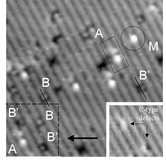
Figure 1. A filled-state STM image of toluene on Si(001) taken after a deposition of 0.1 L. Examples of the different adsorbed geometries are labeled. The inset shows the region enclosed by dashed lines before deposition. A discussion of the adsorbed states is given in the text. The image size is 160 Å × 160 Å, and the sample bias is –1.0 V.
Upon exposing the clean Si(001)-2×1 surface to toluene,
we observe adsorption exclusively on top of dimer rows. The
adsorbed species are distributed randomly on the surface and are
immobile at room temperature. Figure 1 is an image following
deposition of 0.1 L of toluene on a clean Si(001) surface. To aid
in identification of features, an image of this same area was
taken before deposition. Examples of features related to
adsorption of toluene in different geometries are labeled.
Surface defects are also visible as darkened areas. These are
generally dimer vacancies or C-type defects. This is a filled-state image, with a
sample bias voltage of –1.0 V. The primary features are the
states marked A and B, which persist and are very stable. The STM
tip may be used to induce interconversions between them, as
described below. State A appears as a bright "head"
adjacent to a darkened surface dimer followed by a fainter
"tail," which involves the highlighted buckling of
three Si dimers. State B appears as a darkened square of two
dimers inside of which there is a bright dot. This dot may either
be centered across the dimer row (state B) or off to one side
(state B’).
The inset in Fig. 1 demonstrates that state B’ is the result of adsorption on top of a C-type defect rather than a regular segment of a dimer row. The inset is an image before deposition of the region enclosed in dashed lines in Fig. 1. Two C-type defects are visible, as indicated by the arrows. Comparison with the image after deposition reveals that molecules are adsorbed in state B’ on each of these defects. The bright dot in the darkened square of state B’ appears on the same side of the dimer row as the crescent shape of the defect. Also visible after deposition are two molecules adsorbed on clean areas of the substrate, one in state A and one in state B. Nearly half the adsorptions in Fig. 1 are in state B’. The prerequisite C-type defect sites cover only a small percent of the surface. Therefore, significant population of these sites at low coverages indicates that they are preferred over clean terrace sites. At higher coverages, we observe preferential population of state A due to conversion from a metastable initial state, as described next.
Metastable adsorption and conversion
The remaining feature in Fig. 1 is the symmetric bright spot circled in the upper right. While similar to state A, this state has no adjacent darkened dimer or highlighted buckling. We have labeled this state "M" since we find it to be a metastable initial state: it is only observed for a brief time after a new adsorption. We have observed many cases of state M either when imaging immediately after deposition or when occasionally a molecule enters the area being scanned and adsorbs. (The tip must be retracted in order to avoid blocking the deposition, so we do not scan during deposition per se.) Molecules adsorbed in state M either desorb (most likely due to the influence of the STM tip) or convert to state A, typically after just a few images. These results suggest that state M is a type of weakly bound intermediate state in the chemisorption process and is metastable. We routinely observe surfaces at higher coverages dominated by toluene in state A. Preferential population of state A is likely a consequence of adsorption kinetics, since M is only observed to convert to A.
Examples of both conversion from M to A and desorption from M are shown in Fig. 2, two images taken from a longer time series of images. Image (a) shows three molecules adsorbed in the area after deposition of 0.03 L of toluene. Two are in state M and one is in state A. Image (b) reveals that one of the molecules in state M has converted to state A while the other has desorbed.
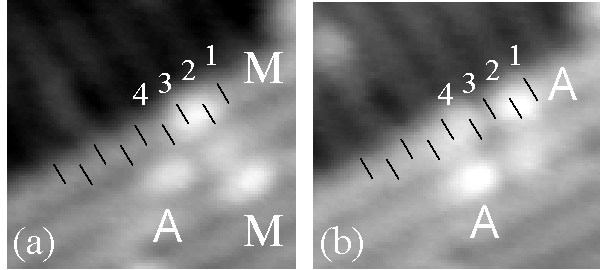
Figure 2. A series of filled-state images showing adsorption in the metastable initial state M and subsequent conversion to state A (upper molecule) or desorption (lower molecule). The conversion from M to A involves a shift of the bright spot in the dimer row direction. State M typically converts or desorbs within a few images after appearing, suggesting that it is metastable and weakly bound. For reference, the positions of surface dimers are marked with black stripes using the frozen-in buckling of dimers along the step edge. The image size is 50 Å × 50 Å, and the sample bias is –1.2 V.
The location of the adsorbed states relative to the underlying surface dimers may be determined by the images shown in Fig. 2. A step edge is visible, and the frozen-in buckling of the dimers along the edge enables us to mark the position of the dimers with black stripes. In image (a), observing the uppermost molecule, we find that the bright spot of state M is centered approximately between two dimers, marked 2 and 3. In image (b), we find that the bright spot in state A is shifted to the upper right along the dimer row from where the bright spot in state M was. This shift along the dimer row, in either direction (as expected by symmetry), is characteristic of all conversions from M to A. Notice the single darkened dimer next to the bright "head" of both examples of state A in (b); the three-buckled-dimer "tails" do not contrast very sharply with the substrate in these images (see discussion of bias dependence below).
Bias dependence of adsorbed states
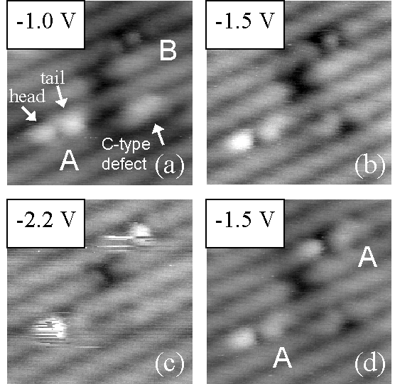
Figure 3.Images showing the filled-state bias dependence of toluene in states A and B as well as a tip-induced conversion from state B to state A (upper molecule) using a high bias voltage. Detailed observations are given in the text. Image size is 50 Å × 50 Å.
Discussion of the bias dependence of the adsorbed states
for toluene will aid in elucidating aspects of the binding of
this molecule to the surface, especially in comparison to
benzene. This is a fruitful comparison because the only
difference between these two molecules is that for toluene a
methyl group is substituted for one of the hydrogen atoms of the
benzene ring. Figure 3 shows the filled-state bias dependence of
states A and B. The four images are taken from a time sequence of
the same spot at different sample bias voltages, which are
labeled in the upper left of each image. The "tail" of
state A is observed to have a bias dependence very similar to
that of the C-type defect.4
At low bias magnitudes, both the tail and the defect are bright
and contrast with the dimer rows (image (a)). Their brightness
decreases as the magnitude increases (images (b) and (c)). Near
–2.2 V, both are indistinguishable from the dimer row (image
(c)). The "head" of state A and the dot of state B both
become puffier in appearance as the bias magnitude increases. All
adsorbed states are very disturbed by high bias magnitudes (image
(c)). Transitions between the states may be induced under these
conditions (see the upper molecule in images (b) through (d)).
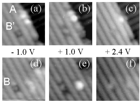
FIG. 4. Figure 4.Images showing the empty state bias dependence of toluene in states A, B, and B’. The top three images are of one area and the bottom three are of another area. Sample bias voltage increases to the right. Image size is 50 Å × 50 Å.
Figure 4 shows the empty-state bias dependence of states A, B, and B’. The top three images are of an area containing molecules in states A and B’. The bottom three images are of an area containing a molecule in state B and C-type defect. (The states B and B’ are sometimes difficult to distinguish in our STM images, depending on the resolution of the tip and choice of bias voltage. In this case, identification was aided by referring to the image before deposition). For comparison, a filled-state image at –1.0 V is shown leftmost for each area. The middle images are at +1.0 V, and the rightmost images are at +2.4 V. For states B and B’ at +1.0 V, the darkened area that spans two dimers in filled-states now spans four dimers. The difference between states B and B’ in empty states at +1.0 V is in the position of the dot: in state B it is off-center and in state B’ it is centered in the dimer row direction. At high positive biases, the dimer rows of the substrate reverse their contrast and appear as dark lines, due to tunneling into the p * states of the dimers.5 In the images at +2.4 V, there are no longer darkened dimers associated with states B and B’, but rather faint dots centered on dimer rows. The buckled "tail" associated with state A is also not apparent at +2.4 V, and this state appears as a bright dot centered on a dimer row.
Comparison to benzene on Si(001)
Unlike toluene, benzene on Si(001) has been studied theoretically.6,7,8,9 The most recent results are in good agreement with experimental observations.6,10,11,12 The calculated atomic structures can account for the appearance in STM images of the adsorbed states of benzene. The states of toluene described here closely resemble those of benzene in STM images.6,10 Therefore, comparison of the appearance of these two molecules on Si(001) provides an opportunity for insight into the atomic structures of toluene on this surface. The benzene states have been labeled A, B, and B’, and our identical labeling of the toluene states reflects similarities in appearance. For both molecules, state A features a symmetric bright spot over one dimer. Benzene has been shown to adsorb intact.11 The calculated models for benzene in state A show a non-tilted molecule bonded to just one dimer and centered over this dimer.6,7,8 A similar scenario may be expected for toluene in state A. However, bonding of this molecule seems to affect several additional dimers as evidenced by the adjacent darkened dimer and three-dimer-long highlighted buckling, which are not observed for benzene.
Further support for this idea is obtained by comparing the states B and B’ observed for benzene and for toluene, which are again very similar. Just as for toluene, filled-state images of benzene states B and B’ (reported by Lopinski et al.) show the darkening of two surface dimers and a dot above them that is either symmetrically or asymmetrically placed depending on whether benzene is adsorbed on a regular segment of a dimer row (B) or on a C-type defect (B’).6 Empty-state images also reveal the darkening of two dimers. This contrasts with our results for toluene shown in Figs. 4FIG. 4. Figure 4(b) and 4(e), where four dimers are darkened. Lopinski et al. calculate atomic structures for benzene states B and B’ and find that the molecule is bonded in tilted configurations that bridge two dimers.6 The molecule has four of its neighboring C atoms bonded to the four Si atoms of the dimers, which appear darkened due to this bonding. The other two C atoms of the molecule share a double bond, proposed to be responsible for the bright dot in states B and B’. The placement of the dot in images is explained by rotating the structure for state B by 90 degrees to get B’. By analogy we may speculate that toluene states B and B’ are bridging configurations, but that interaction with more than two dimers is involved. The fact toluene interacts with more surface dimers than benzene may be attributed to the methyl group in the structure of toluene, the presence of which distinguishes toluene from benzene.
Our images of state M reveal that the structure for this state must place the molecule between two dimers as in states B and B’. Unfortunately we cannot offer detailed atomic models of the adsorbed states of toluene on Si(001). Further insight into the geometry of these states must await theoretical study or experiments using spectroscopic techniques.
Thermal decomposition and formation of SiC clusters
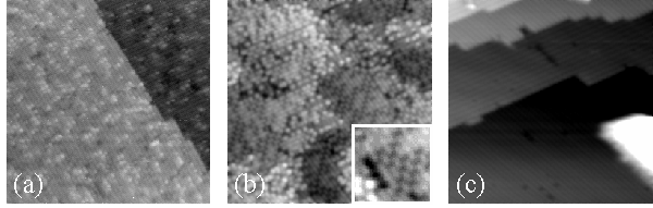
Figure 5.Images demonstrating the results of annealing toluene on Si(001). Image (a) was taken after deposition of 0.25 L of toluene at room temperature. Image (b) was taken after annealing at about 700 °C for 5 minutes. Domains of c(4×4) ordering (see inset for a detailed view) and disordered step edges are observed. Image (c) was taken after an additional anneal near 1000 °C for 15 seconds. A large SiC cluster is visible in the lower right. These clusters are separated by clean areas displaying the normal (2×1) surface structure. The image size is 400 Å × 400 Å. The sample bias is –2.0 V.
Figure 5 is a series of images showing the behavior of the toluene/Si(001) system upon annealing. Image (a) shows a room temperature deposition of 0.25 L. Image (b) shows the result of a subsequent anneal for 5 minutes at 700 °C. Toluene molecules decompose upon annealing to this temperature. Some of the molecular fragments desorb, as evidenced by a small pressure spike during the anneal. These fragments are most likely H atoms. Other fragments, most likely C atoms, incorporate into the surface. This results in highly disordered step edges and local patches of c(4×4) ordering, shown in more detail in the inset of image (b). The c(4×4) phase is known to be a metastable phase of the Si(001) surface and has been induced in a number of ways, all of which involve annealing in the temperature range » 600-700 °C.13 One of the principal techniques has been to anneal the surface after adsorbing molecules that act as a source of C atoms, such as acetylene or ethylene.14,15 Apparently toluene performs the same role in our experiments. Image (c) shows the surface after an additional anneal for 15 seconds at 1000 °C. The (2×1) ordering returns to the terraces at this temperature, and the step edges revert to the usual structure. However, we also observe large clusters of SiC. Part of one such cluster is visible in image (c) in the lower right. Presumably, carbon atoms that were formerly spread out over the surface are now collected in these clusters along with Si atoms from the surface. These clusters are isolated and separated by clean areas, are generally rectangular in shape, and can pin step edges in place. Similar results were obtained by annealing acetylene on Si(001) at about 1000 °C.14 In the acetylene experiment, the clusters were determined to be SiC, as indicated by the presence of the Si-C stretching mode in the HREELS spectrum. The decomposition of toluene on Si(001) indicates that this molecule, like acetylene and ethylene, may be suitable as a source of C atoms in chemical vapor deposition film growth processes.
These results differ distinctly from the annealing behavior of benzene on Si(001). We find that benzene desorbs completely upon annealing above 250 °C, leaving behind a clean (2×1) surface. Thermal desorption spectra obtained by Taguchi et al. indicate that benzene desorbs intact.11 The fact that toluene instead decomposes suggests that this molecule is more strongly bound to the surface than benzene. This conclusion is supported by the results of bias-dependent imaging discussed above, which indicate that more Si dimers are involved in binding toluene to the surface than for benzene.
We have conducted a preliminary investigation of the adsorption and thermal decomposition of toluene on the Si(001) surface. Adsorption occurs only on top of dimer rows. Several adsorbed geometries are observed. A metastable and weakly bound initial state, M, converts exclusively to state A. The two primary states, A and B, have been characterized. Conversions between them may be induced by scanning at high bias voltages. Insight into the adsorbed geometries has been obtained by comparison to benzene on Si(001), whose adsorbed states closely resemble those of toluene in STM images and have been extensively studied. While benzene has been shown to interact with either one or two surface dimers, evidence that toluene interacts with more than two dimers is found in the bias dependence of the states. Toluene decomposes upon annealing. A c(4×4) phase is induced at 700 °C and formation of SiC clusters occurs at temperatures near 1000 °C. These results indicate that toluene may be used as a source of carbon atoms in chemical vapor deposition film growth.
References
1 J. T. Yates Jr., Science 279, 5349 (1998).
2 J. S. Hovis and R. J. Hamers, J. Phys. Chem. B 101, 9581 (1997).
3 Silicon Carbide and Related Materials, Eds. M. G. Spencer, R. P. Devaty, J. A. Edmond, M. Asif Khan, R. Kaplan, and M. Rahman (Institute of Physics, Bristol and Philadelphia, 1994).
4 R. J. Hamers and U.K. Kohler, J. Vac. Sci. Technol. A 7, 2854 (1989).
5 J. A. Kubby and J. J. Boland, Surf. Sci. Rep. 26, 62 (1996).
6 G. P. Lopinski, T. M. Fortier, D. J. Moffatt, and R. A. Wolkow, J. Vac. Sci. Technol. A 16, 1037 (1998).
7 U. Birkenheuer, U. Gutdeutsch, and N. Rösch, to appear in Surface Science.
8 H. D. Jeong, S. Ryu, Y. S. Lee, and S. Kim, Surf. Sci. 344, L1226 (1995).
9 B. I. Craig, Surf. Sci. 280, L279 (1993).
10 B. Borovsky, M. Krueger, and E. Ganz, Phys. Rev. B 57, R4269 (1998).
11 Y. Taguchi, M. Fujisawa, T. Takaoka, T. Okada, and M. Nishijima, J. Chem. Phys. 95, 6870 (1991).
12 S. Gokhale, P. Trischberger, D. Menzel, W. Widdra, H. Dröge, H. -P. Steinrück, U. Birkenheuer, U. Gutdeutsch, and N. Rösch, submitted to J. Chem. Phys.
13 R. I. G. Uhrberg, J. E. Northrup, D. K. Biegelsen, R. D. Bringans, and L. –E. Swartz, Phys. Rev. B 46, 10251 (1992).
14 L. Li, C. Tindall, O. Takaoka, Y. Hasegawa, and T. Sakurai, Phys. Rev. B 56, 4648 (1997).
15 T. Takaoka, T. Takagaki, Y. Igari, and I. Kusunoki, Surf. Sci. 347, 105 (1996).
We thank the National Science Foundation for support under grant DMR-9614125.
Jump to
Hot STM Labs
Benzene