Adsorption of TiCl4 and Ti growth on Si(001) were investigated over a range of temperatures by scanning tunneling microscopy. At 300 K, intact TiCl4, Ti and Cl, and mobile TiCl2 are identified on the Si surface. At higher temperatures, deposition initially produces two-dimensional Ti islands, and continued deposition produces three-dimensional clusters. Above 630 K, both Si and Ti islands and Si/Ti clusters are formed.However, cluster growth is limited by Cl passivation of Si and Ti surfaces below 950 K. Above 950 K, the tops of partially submerged titanium silicide crystals are observed.
___________________________________________
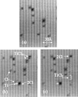
Figure 1. A sequence of STM images showing adsorption of TiCl4 on a Si(001) surface at 300 K. (a) A bare surface before the dose,(b) after the dose, TiCl4, Ti and Cl are observed. (c) Twenty seconds later, TiCl4 has dissociated into TiCl2 and 2Cl. The sample bias voltage is –2.0 V.
We identify TiCl4, TiCl2, Ti, and Cl on the clean Si(001) surface by analyzing STM images before and after several instances of dosing surfaces with a fraction of a monolayer of TiCl4.
|
Typical images are shown in Figure 1. The same area of a 300 K Si(001) surface is imaged before (1a) and after (1b) exposure to 0.05 L of TiCl4, and again 20-seconds later (1c). The arrows in Figs. 1b and 1c highlight four different adsorption features observed.
Ti and Cl are identified by comparing our STM images at various biases (not shown) with previous STM studies of PVD of Ti on Si (001)[i] and the chemisorption of Cl and CH3Cl on Si(001)at room temperature.[ii] Cl adsorbs singly on individual substrate atoms; usually 2 Cl atoms adsorb on adjacent Si atoms. All three types of Cl adsorption features identified by Boland are observed.12,[1] Figure 1b shows that the Ti has adsorbed on a pedestal site near a single dimer vacancy between two neighboring Si dimers in the same row. At a –2.0 V sample bias, a single adsorbed Ti atom appears as a 0.6 ±0.1 Å high protrusion with a diameter of 8 ± 0.5 Å.
The two other adsorption features cannot be identified with either Ti or Cl. Conversions between these and Ti and Cl features allow their identification as intact TiCl4 and the fragment TiCl2. Over a period of a few minutes, TiCl2, Ti, and Cl replace the initial density of TiCl4. Through successive images, we see TiCl4 disappear, leaving 2 Cl and a white streak along a substrate row. In every instance investigated (around 30) the creation of a streak is simultaneous with that of a pair of Cl atoms on the same or an adjacent substrate row. A streak is produced by a mobile species moving slightly faster than the STM scan rate.[iii] An example of such a conversion can be seen in fig’s 1b and 1c. In fig. 1b, taken immediately after a dose, two features are labeled TiCl4. Figure 1c shows that, twenty seconds later, 2 Cl’s and a white streak along the same dimer row have replaced one of these features. On four occasions individual streaks have been observed to transform into a single Ti atom and 2 Cl atoms near a defect. Thus, we identify the streaks with mobile TiCl2 molecules and propose the following decomposition path:
|
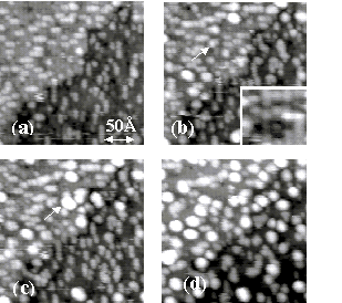 |
Figure 2. A
sequence of STM images of a Si(001) surface at 475 K. (a) After an initial exposure
to TiCl4 (0.2 L). Ti forms
one-dimensional islands. Cl
adsorption produces dark surface regions. (b) After a second dose of
TiCl4 (0.4L), 90% of surface is covered by Ti and Cl. The arrow indicates a mobile
Ti atom on an island. The gray scale in the inset has been
exaggerated to assist identification of the different surface
features: white is a Ti
atom, light gray is bare Si surface, dark gray is Cl covered
surface, and black is a surface vacancy. (c) After a 1-minute
interval, ripening is observed.
A typical cluster has a height of 2.7 Å. (d) After a further dose of
TiCl4 (0.9 L). The sticking
probability has decreased from unity.
The number of 4.2 Å clusters increases by a factor of three. The sample bias voltage is
–1.6 V.
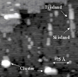 |
Figure 3. An STM image showing both Si and Ti islands on a Si(001) surface at 630 K. The sample bias voltage is -2.5V.
|
Figure 3 shows the Si, Ti, and Si/Ti islands and clusters present on a 630 K Si(001) surface that has been dosed with 0.1 L of TiCl4. The Si islands are identified by image comparison with Si PVD on Si(001) studies and images of roughly annealed bare Si(001).[ii] At this temperature, two mechanisms can supply the Si ad-atoms incorporated in these features. Silicon atoms along the step edges can escape onto the terraces,15 and Si atoms in the terrace surfaces can be ejected and replaced by Ti atoms.[iii] After the dose, only half of the expected Ti was observed; assuming that the sticking probability is roughly the same as on the 450 K surface, the other half of the Ti atoms must have sunk into the Si substrate by this process. Once on the terraces, Si and Ti are mobile at 630 K, and can meet to form the observed features. 16,13 A uniform fuzziness observed in the images may be due to the presence of highly mobile Cl.
Analyzing the islands and clusters, a few observations can be made. These features often abut surface defects, suggesting that the defects may influence the seeding or limiting of growth. Also, image series reveal that these features are stable, in spite of a measured rate of Ti diffusion into the surface near 4 Hz at this temperature.11 This indicates that the diffusion barrier is increased either by island formation or possibly by the presence of Cl on the surface. The average cluster height is 6 ± 0.4 Å.
Previous work has determined some of the details of Ti CVD from TiCl4 at high temperatures. In LEED, TPD, and AES studies, Medicino and Seebauer concluded that Cl-free material is difficult to grow using TiCl4 below 950 K.4 However, Hocine and Mathiot found that, above 950 K, Ti diffuses rapidly into the Si,[iv] thus making the precursor better suited for silicide than for thin film growth. Indeed, Briggs et al. have recently used STM and Transmission Electron Microscopy (TEM) to investigate titanium silicide produced by a TiCl4 dose and an anneal to 1200 K.9 Additionally, it is known that Cl etches the Si(001) surface and produces SiCl2 gas above 800 K; during the etching processes, ragged step edges, pits, and 2D islands form on the Si(001) surface.[v]
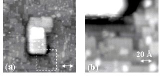
Figure 4. STM images obtained after exposing a Si
(001) surface at 970K to TiCl4. (a) A TiSi2 structure
surrounded by a characteristic Cl etched surface. (b) A
close-up of the edge of the structure reveals a trough circling
it. The sample bias voltage is –2.1 V.
As
expected, after exposure to 1.5L of TiCl4 at 970 K, the surface has the
ragged appearance characteristic of Cl-etched Si(001)18 and is populated with
structures such as that in Fig. 4.
These cover approximately 3% of the surface. Focusing on the edge of the
structure shows that it grows into the Si substrate, as is seen in Fig. 4b. Immediately surrounding it, there is a trough, more than 5
atomic layers (6.8Å) deep. This
results from Si being gathered into the structure during its
formation. The well-defined
geometry of these structures indicates that they are crystalline. Indeed, we expect titanium
silicide crystal formation at this temperature. Theory predicts that the most
likely equilibrium stochiometry is TiSi2 in the C49
structure,[vi] and
recently Briggs et al. verified this for samples exposed
to either pure Ti or TiCl4 and well annealed at 1200
K.9
The structures seen in that work display the same geometries
and surrounding troughs as those seen here. While the visible height of
the structure in Fig. 4b is 14 ± 0.5 Å, TEM images reveal that
the TiSi2 crystals in Brigg’s work extend
“like icebergs” deep below the surface with widths only
a few times greater than their depths.9 A
further 2L dose of TiCl4 doubles the number of titanium
silicide structures and the average visible height of TiSi2
grows up to 20Å, while the step edge recession is more than 7
atomic layers (9.5Å).
At 300 K, we observe intact TiCl4 and mobile TiCl2 as well as Ti and Cl atoms on Si(001). Initially TiCl4 dissociates into TiCl2 and 2 Cl atoms. Next, some of the TiCl2 dissociates near vacancies into Ti and 2 Cl atoms. However, the complete decomposition is slow at this temperature. For deposition at 450 K, we observe 2D Ti island growth followed by Ti clustering. Dosing at 630 K, conglomerate islands and clusters of Ti and Si form. At 970 K, just above the Cl-free temperature, Cl etches the surface and partially submerged TiSi2 crystals are formed locally.
[1] The slight deviation from the expected ratio of 1 to 2 is likely due to the difficulty in distinguishing Cl pair features from surface defects.
[2] The observation of roughly 400 Ti atoms for 10 min. yields only 4 candidates for Ti diffusion beneath the surface. This suggests a rate of less than 1.5 × 10⁻⁵ Hz.
[i] T. Mitsui, R. Curtis, and E. Ganz, J. Appl. Phys. 86, 1676 (1999).
[ii] C. Pearson, M. Krueger, R. Curtis, B. Borovsky, X. Shi, and E. Ganz, J. Vac.
Sci. Technol. A 13, 1506 (1995).
[iii] K. Miwa and A. Fukumoto, Phys.
Rev. B 52, 14748 (1995); B. D. Yu, Y. Miyamoto, O. Sugino, T. Sakai, and T. Ohno, Phys. Rev. B 58, 3549 (1998).
[iv] S. Hocine and D. Mathiot, Mater.
Sci. Forum 38-41, 725 (1989).
[v] M. Chander, D. A. Goetsch, C. A. Aldao, and J. H. Weaver, Phys.
Rev. B 52, 8288 (1995); K. Nakayama, C. A. Aldao, and J. H. Weaver, Phys. Rev. B 59, 15893 (1999); G. A. deWijs, A. DeVita, and A. Selloni, Phys. Rev. Lett. 78, 4877 (1997).
[vi] X. Wallart, J. P. Nys, and G. Dalmai, Appl. Surf. Sci. 38, 49 (1989); X. Wallart, J. P. Nys, H. S. Zeng, G. Dalmai, I. Lefebore, and M. Lannoo, Phys.
Rev. B 41, 3087 (1990); H. Jeon and R. J. Nemanich, Thin Solid
Films 184, 357 (1990); B. D. Yu, Y. Miyamoto, O. Sugino, T. Sasaki, and T. Ohno, Appl. Phys. Lett. 72, 1176 (1998).
[1] Cl appears either individually or in pairs, oriented either parallel or perpendicular to the substrate dimer rows. Though Cl pairs resemble common surface defects, they may be distinguished at low sample biases. Also, continuous patches of Cl pairs display dim dimer rows parallel to the surface rows where as patches of dimer vacancies reveal the perpendicular rows of the next Si layer down.
[i]
K. Ishiyama, Y. Taga, and A. Ichimiya, Phys. Rev. B 51, 2380 (1995); K. Ishiyama, Y. Taga, and A. Ichimiya, Surf. Sci. 349, 267 (1996); K. Ishiyama, Y. Taga, and A. Ichimiya, Surf. Sci. 357-358, 28 (1996).
[ii]
J. J. Boland, Science 262, 1703 (1993); M. J. Bronikowski and R. J. Hamers, J. Vac.
Sci. Technol. A 13, 777 (1995).
[iii] M. Krueger, B. Borovsky, and E. Ganz, Surf. Sci. 385, 146 (1997).