Nanolithography by selective physical vapor deposition of Palladium with an atomic hydrogen resist
We investigate selective Palladium Physical Vapor Depoision (PVD). Since the maximum thickness of well-defined silicide features is limited by the selectivity of the deposition process[1], we investigate the dependence of selectivity on deposition temperature. Upon Pd PVD on an STM patterned monohydride terminated Si(001)-(2×1) surface, we find that Pd growth selectivity is due to the different diffusion lengths on bare and H terminated surfaces, and that the selectivity increases with increasing temperature from 500 K to 600 K. A crystal structure is observed after a 1000 K anneal.
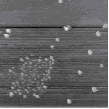
Figure 1. Palladium deposition on hydrogen terminated and bare regions of a Si(001) surface at 533 K. The pollygon in the lower left is the bare region.
The differences between Pd deposition on bare and on H terminated Si(001) are investigated by dosing a patterned surface; an example is seen in Figure 1. We find that the volumetric ratio of material on the bare surface to that on the hydrogen terminated surface is 1.3 ± 0.5, which is consistent with equal sticking probabilities. However, the distribution on these two surfaces differs greatly. Specifically, the clusters are smaller and denser on the bare surface. Also, there is a significant Pd enhancement along the H terminated – bare region border. This enhancement border, approximately 5 nm wide, is presumably where Pd that originally deposited on the H terminated surface diffused onto the more reactive bare surface. These observations suggest that the Pd diffusion length is greater on the H terminated surface than on bare silicon.
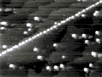
Figure 2 Palladium selectively deposited on a 6nm wide strip of bare Si(001) on a H terminated surface at 575 K.
The existence of an enhancement border indicates that substantial selectivity can be achieved on its length scale, 5nm. Figure 2 shows an example of features resulting from selective Pd deposition on a 575 K surface. We find that the selectivity increases with increasing temperature: 20:1 at 525 K, 35:1 at 550 K, and 50:1 at 575 K. Attributing the selectivity to a difference in diffusion lengths, this temperature dependence could reflect the increase in this difference with temperature. In each case, the clusters along the line are of uniform spacing and volume.
A previous study performed under similar experimental conditions indicates that these clusters are Pd2Si. With further deposition, Pd2Si clusters grow according to the Volmer-Weber mode. We observe that sequential dosing causes uniform growth of the original clusters and negligible formation of new ones. This and the relatively high selectivity at 575 K suggest that a continuous wire could be grown upon further dosing. The clumpy growth has one notable drawback: as each cluster’s growth is symmetric over its surface, a continuous wire’s cross-section will be far from uniform; in fact, the thinnest continuous wire will be composed of clusters whose diameters equals the maximum separation of the initial cluster sites. However, it is possible that post deposition annealing could cause more uniform silicide formation.
Figure 3. Palladium Silicide crystal formed on the Si(001) surface after annealing to 1000 K.The dashed hexagon emphasizes the symmetry of the surface reconstruction.
After annealing to 1000 K, small crystallites are observed. Such a structure is seen in Figure 3. Because Pd silicides are known to form in this temperature range, we expect that these are silicide; however, the exact stochiometry has not been identified. The crystallites exhibit atomically flat plains with a 0.5 ± 0.2 Å vertical corrugation which defines an imperfectly periodic diamond unit cell with 17 ± 1 Å sides and an acute angle of roughly 60°. One cell is outlined in Fig. 3. The crystallites are approximately 20 Å tall and have a terrace step-height around 5 Å. The exact origin of hexagonal features in the crystal is uncertain; however, the influence of the surface geometry cannot be ruled out.
[1] More selective systems accommodate higher doses before off-pattern growth causes significant feature degradation.
We would like to thank the National Science Foundation for support under Grant No. DMR-9980295.
Jump to
Copyright 1998 by the Regents of the University of Minnesota, Dept. of Physics & Astronomy. All rights reserved.